ADC is an irresistible topic for a Nyquist ADC designer. Several years ago I touched a bit of it when I studied noise-shaping SAR ADC. Recently I have the opportunity to revisit this topic.
The good thing is that there are plenty of resources you can find from the internet; while the bad part is that after reading so much stuff it seems what I know about it is still these two curves… Frustrating!
Fig.1 STF and NTF of ADC
In this post, the focus is not on the technical details of ADC design, but on sharing my experience of getting started with it. Mainly I will point out the good references which speed up my learning curve and prevent drowning in the ADC sea of knowledge.
First, textbooks.
The popular yellow and green bibles are too difficult to digest for a newbie (BUT bibles are bibles! You will still need them time after time…). Until I found the data converter book written by Prof. Franco Maloberti, I just can’t stop reading its chapter 6 on oversampling and low order modulators. Besides a good explanatory flow, it also provides Matlab/Simulink models to vividly show the working algorithms and circuit defects of low order ADC.
cppsim.com by Michael H. Perrott. I benefit a lot from one of his tutorial (accessed 06/02/2022) on “Behavioral Simulation of A Second Order Discrete Time Delta‐Sigma ADC Using CppSim”. At the end of the document, there is an appendix on Matlab synthesis code based on Schreier’s Delta-Sigma Matlab Toolbox (very handy!).
Finally, I know … again … too much info here. Then stop reading, just start to create some behavioral model first!
Fig.3 My memo on design procedure of Delta-Sigma ADC (copied from one of Prof. Temes’s lecture notes)
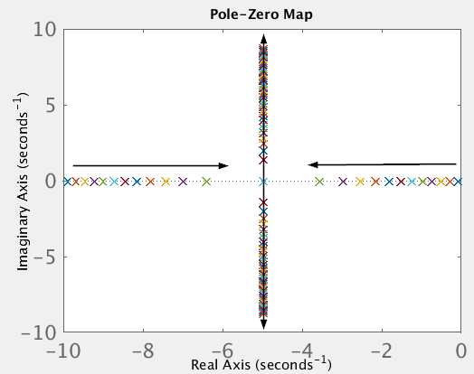
Smith chart is used be mysterious to me. My daughter has an interesting book named my heart is like a zoo. This makes me come up with the story – my circle is like a Smith chart.
Figure 1. My circle is like a Smith chart
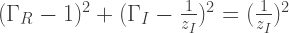
I can find lots of reference on Smith chart online, among which one of the most useful one is explained by Prof. F. Delssperger and he also develops a handy software to help us with matching and etc. After reading his slides, I kind of understand that Smith chart is trying to combine the impedance in Z plane with the reflection coefficient in Polar diagram. However, I am still confused about the exact size and position of the circles until I happen to find this derivation.
I extract the main flow of derivations here. For details, please click the above link.
Second, this coefficient corresponds directly to a specific impedance as seen at the point it is measured. It can be calculated based on a load impedance ZL (using a reference impedance Z0). And the load impedance is further normalized to the reference impedance zL=ZL/Z0.
Third, the normalized load impedance, which is also a complex number, can be expressed by the reflection coefficient.
Fourth, after rationalizing, the normalized load resistance zR and load reactance zI can be expressed by the following two circle equations.
Finally, thanks to the author’s derivation, the equations of the two circle can be rewritten in a familiar format.
It’s a rather old topic and one can find many good references. In this post, I will write down some of my basic understandings on this circuit.
Operation of CML latch
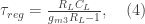
Figure 1 shows a simplified block diagram of divider-by-2 and a CML (current-mode logic) latch. M1/M2 form a preamplifier and M3/M4 a cross-coupled pair. Fig. 2 illustrates the low-frequency and high-frequency operation of CML latch. During the low-frequency operation, when CK is high, the input is amplified by M1/M2; when CK goes low, the cross-coupled pair performs regeneration and latches the state. For short cycle operation, the cross-coupled pair continues to provide gain in the store mode, regenerating to a final differential output of Iss*RL. This condition is met if gm3RL>1.
Fig.1 A divider-by-2 and a CML latch [1]Fig.2 Low-frequency and high-frequency operation of CML latch [1]
Speed estimation of CML latch
When CK is high, the circuit can be viewed as a single-pole amplifier. Assume that a step voltage is applied at the input, the differential output voltage can be expressed as
where VXY0 and VXY1 are the initial and final differential output during the sense phase, gm1 is the transconductance of the input transistor, the product of RL and CL is the time constant. RL and CL are the equivalent resistive and capacitive load seeing from node X/Y.
As is shown in Fig.2, in a divider-by-2, input of one latch is output of the other. Both the initial differential voltage at X/Y (VXY0) and the input voltage step (Vstep) have the same value of Iss*RL. Replacing VXY0 and Vstep with Iss*RL, Eq(1) can be rewritten as
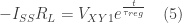
When clock goes low, the latch starts regeneration and the differential output continues to evolve, which can be expressed as
The regenerative time constant equals
where gm3 is the transconductance of the cross-coupled pair. The latch regenerates the differential output to a final value of -Iss*RL. Replacing VXY2 with -Iss*RL, Eq(3) can be rewritten as
Now we have derived the amplification time, Eq(2), and the regeneration time, Eq(5), respectively. It would be interesting to visualize them in the following plots (Fig.3 and Fig.4). It can be seen that the optimal speed happens when the differential output at the end of the sense phase (VXY1) is between its final settled value and half of it.
Fig.3 Estimated speed of CML latch with small capacitive load (10fF)
Fig.4 Estimated speed of CML latch with large capacitive load (50fF)
The above plots are based on the following assumptions:
Gm/Id: a value of 10 is a good start. This indicates that operating the transistor in moderate inversion is optimal when we value speed and power efficiency equally. The conversion between Gm/Id and inversion coefficient(IC) can be referred to this post.
Gain (G): a value around 3 is a good start. For submicron CMOS node, the self-gain of a standard transistor with minimum length is normally no large than 10. In this case, we further assume M1/M2 and M3/M4 have the same size.
Differential output voltage (Iss*RL): in the range of 400 ~ 600 mV [2].
Tail current (Iss): assume RL is 500Ohm, Iss around 800uA is a good start point. Then gm = Gm/Id*(Iss/2) = 10*400uA = 4 mA/S. (Note that gmRL > 1 holds)
Transistor width (W): according to gm/Id simulation of a minimum-length transistor in submicron process, for 1-um width a gm/Id of 10 needs ~150-uA bias current. If the width is 4x, the bias current will be 600uA.
Capacitive load (CL): the capacitive load contributed by the transistors are equal to 2*Cgg+2*Cdd ~= 3Cgg. With width of 4um and length of 30nm, the Cgg can be approximated to about 2.4fF (4*0.03*20=2.4fF). Normally, the load from a succeeding buffer will dominate.
The Matlab script used to plot the data can be found here.
Doping is a technique used to modify the density of charge carriers in semiconductors. A small section of the periodic table is copied as follows.
Boron is a “Group 3” element. It has 3 valence electrons in its outmost shell. Once it is introduced into the silicon lattice it will bond to the nearby silicon atoms with the traditional double bonds, and produce a hole which will accept electrons and migrate around. The hole concentration (p) is approximate to the density of Boron atoms.
Phosphorus is a “Group 5” element. It has 5 valence electrons in its outmost shell. Once it is bonded to the nearby silicon it will produce a free electron and the electron acts as a donor. The electron concentration (n) is approximate to the density of Phosphorus atoms.
Note that the product of n and p is constant, which is equal to ni2.
Finally, an interesting question quoted from Prof. Razavi’s Youtube video on Electronics: Q: What happens to n and p in n-type silicon as T increases? A: n keeps constant and p increases as T increases.
In reality, there are no holes! It just refers to positive charge.
The diagram below shows positive charge travels from the left to the right of silicon. At t1, one electron is released which produces a positive charge (indicated as a hole); at t2, the second electron is released and trapped in the hole shown in t1; at t3, the third electron is released and again trapped in the hole shown in t2.
This explains why movement of holes is shower than that of electrons.
For pure silicon, the density of holes is equal to the density of electrons (ni).
A silicon atom has 14 electrons. In its outmost shell, it has 4 valence electrons.
Covalent bonding in silicon:
Its resistivity drops as temperature rises.
Density of free electrons in silicon can be calculated as:
At T=300K,
In the same cubic, there are 5×10²² silicon atoms. The ratio of electrons to silicon atoms is tiny tiny…Hence we need to do something to make it conducting.
Most of the information is gathered after watching the youtube video from Prof. Behzad Razavi’s Electronics 1. He is really talented at explaining things. If you have time, just skip mine and watch his video.
Feng Tang once said that if you want to know a bit about a new field, go and find 100 keywords. Digest them in two or three days, and you will look like a professional.
Somewhat make sense!
This triggers me to think about the keywords in my field – IC design. Astonishingly, some words are so common to me but I can’t tell the real details. Am I already a professional?! Maybe I can start a similar project in the dark cold Covid nordic winter to cheer up a little bit 🙂
100 is not an absolute number to target, but in the beginning, let’s say 100. In addition, two or three days is also mission impossible for me, maybe two or three years…
Just some basic understandings on analog filters which is inspired by ‘The Guru’ in our company. To clarify my thoughts, I will write in the format of Q&A. There are four questions to answer:
What do we dream for a low-pass (LP) filter?
Why complex poles are required?
How to generate complex poles without inductor?
Any real-life example?
Q1) What do we dream for a low-pass (LP) filter?
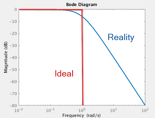
An ideal one, which has a brick-wall response. We only receive what we intend to receive, pure and loss-free. But, in reality…
Fig.1 Brick-wall response (in red) Vs. reality (in bluish)
Q2) Why complex poles are required?
Complex poles help to lift up the magnitude around the cut-off frequency by contributing larger pole quality factor (Q).
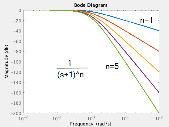
If we only have real poles, though higher-order gives better roll-off, the loss of magnitude around cut-off frequency becomes bigger.
Fig.2 A system from order 1 to 5 which only have real poles
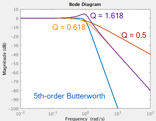
Now we move to a system which has complex poles. Taking the 5th-order Butterworth filter as an example, which has a real pole and two pairs of complex poles, the complex poles with a Q of 1.618 help to compensate the loss of magnitude around cut-off frequency. It tries to approximate the brick-wall response.
Fig.3 Generating 5th-order butterworth lowpass by multiplying (cascading) three transfer functions (1 one-pole + 2 biquads)
Q3) How to generate complex poles without inductor?
The answer is Feedback! R and C only generate real poles. When feedback is applied around a system containing real roots, the closed-loop transfer function may contain complex roots.
Let’s think of this example: an amplifier with two poles. Its transfer function can be written as:
.
The poles are generated by Rs and Cs in the amplifier and they are real. Now assume a negative feedback of beta is placed around the amplifier. The closed-loop transfer function becomes:
.
We can then calculate the two poles of the closed-loop transfer function:
.
By increasing , complex poles can be achieved!
Fig.4 An illustration example of root-locus of poles when A*beta is increased from 0 to infinity
Q4) Any real-life example?
Of course. Fig.4 shows the Two-Thomas biquad. Without the feedback resistor R2, the open-loop transfer function has two real poles: one pole generated by R3 and C1 and the other pole at origin. With a feedback resistor applied, the two poles will move towards each other, arrive at the same position, and then leave the real axis, becoming complex poles.
Fig.4 The common Two-Thomas biquad filter (Wikipedia)


 ADC
ADC


 .
. .
. .
. , complex poles can be achieved!